Semiconductor inspection equipment
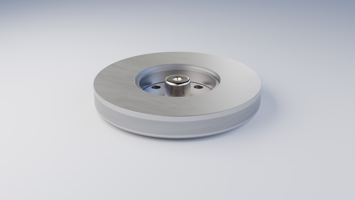
Recently, MPS Microsystems has specialized in the ultra-clean manufacturing and assembly of multi-layer components for semiconductor inspection equipment. These components drastically speed up the inspection of reticles and wafers, critical components in the explosion of demand for electronic devices. Used in an ultra-high vacuum environment, these systems require exceptional cleanliness.
To meet the expectations of the demanding semiconductor and electronics markets, several operations on these critical components are carried out in our ISO 5 clean room. After the different layers have been brazed, the parts achieve the required degree of cleanliness through ultra-high vacuum (UHV) bake-out process and GC-MS analysis. Once magnetized, they are assembled on a ceramic plate with a precision of ± 2 µm.
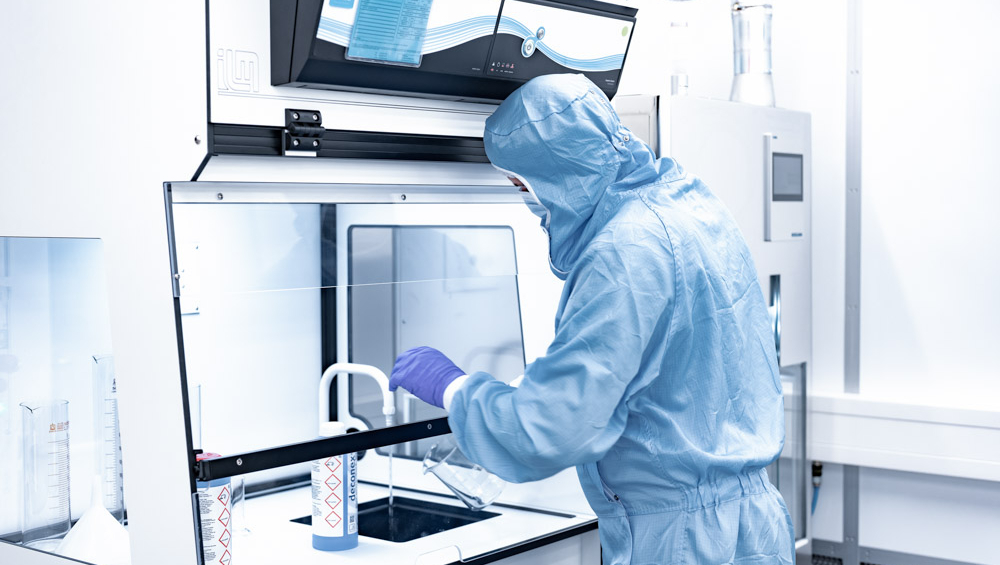
Since 2023, MPS has been operating an ISO 5 clean room for the assembly of ultra-clean components. Custom-designed to meet the high standards of the semiconductor and electronics industries, it is essential equipment for preventing the contamination of delicate parts.
In this room, where particle density and organic contamination are extremely low, we perform operations such as brazing, ultra-high vacuum (UHV) baking, GC-MS analysis, magnetization, and much more.