
MPS Microsystems develops advanced components and systems for various demanding applications in the field of semiconductor. Our expertise in manufacturing, assembly, and cleanliness makes our solutions indispensable assets in our customers' semiconductor inspection and wafer processing equipment.
We manage complex projects from concept to mass production and work with our extensive network of reputable partners to deliver systems that push the boundaries of what is possible. This enables us to provide customized solutions that stand out for their precision, dynamism, and cleanliness.
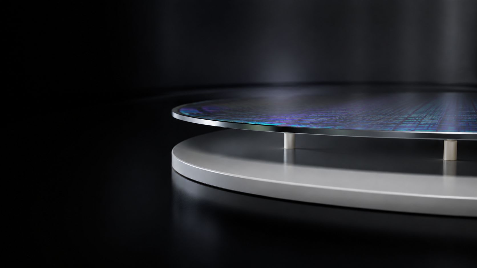
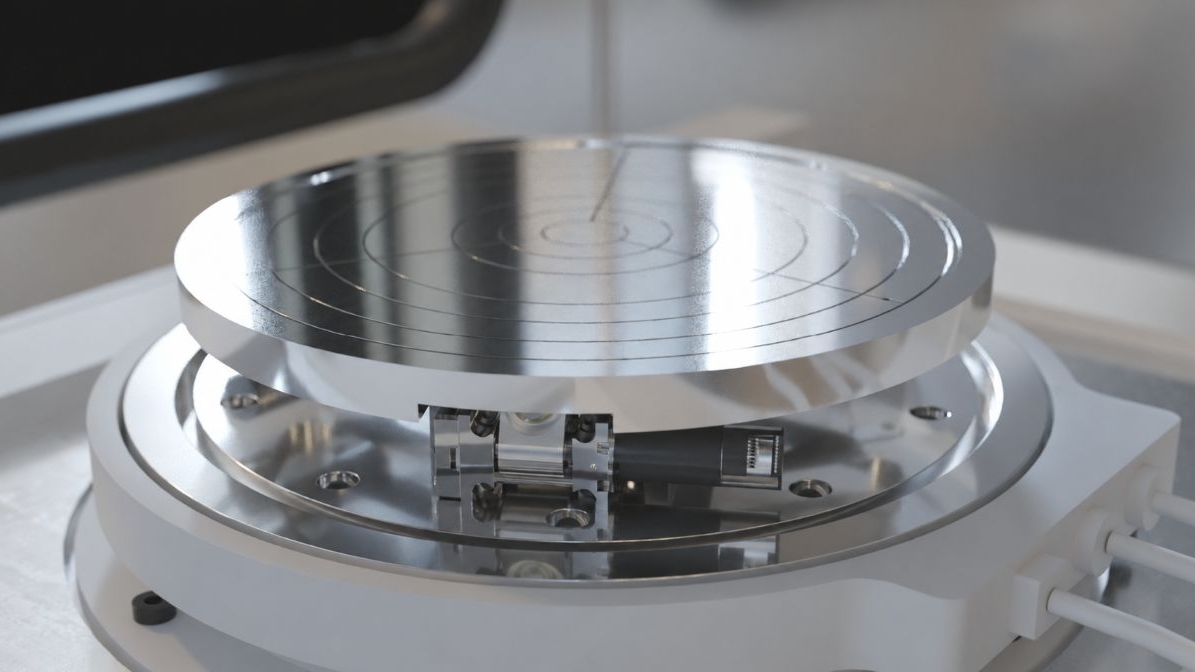
Integrating the mechanism, actuation, and position feedback into a single system, MPS develops wafer and pedestal lift and alignment systems with up to 6 axes and positioning accuracy of ±1 µm. Each motor drives a cam to adjust the height and tilt. The wafer and pedestal positioning system is designed to produce a stroke of ±2 mm and a tilt of ±2°.
The design accounts for payload, travel and positioning requirements within the available space. Particular attention goes to the parts exposed to vacuum or temperature changes, and to the mechanical and control interfaces with the tool.
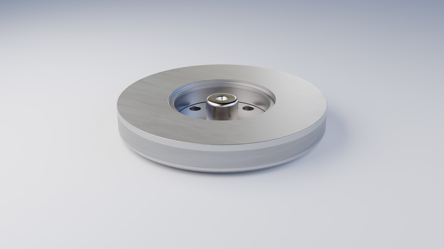
Our work on multilayer magnetic-lens assemblies brings together precision manufacturing and clean micro-assembly for semiconductor inspection. We apply that experience to component and assembly requirements in and around electron-beam columns. The scope can cover manufacturing to your drawings or developing the processes needed to achieve the required geometry and cleanliness.
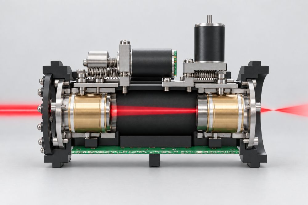
Our coaxial and voice-coil platforms provide a strong base for custom lens-positioning subsystems in semiconductor inspection and metrology heads.
Your optical layout and moving mass guide the choice of mechanism. We develop the guidance, drive and feedback around the required travel and settling time, with particular attention to unwanted lateral or angular movement.
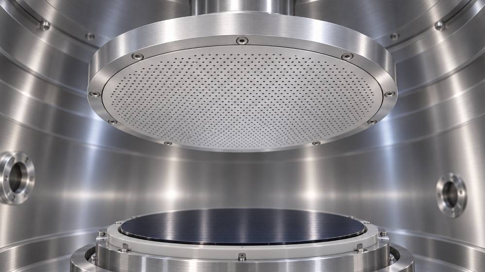
Our precision machining and finishing capabilities are available for wafer processing chamber parts with close-tolerance interfaces or demanding surface requirements like showerhead plates.
Starting from your drawing or component requirement, we review the geometry, materials and process exposure to establish a suitable production route.
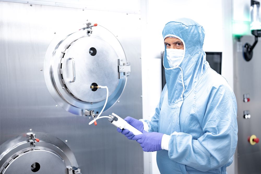
Assembly in ISO 5 and ISO 7 cleanrooms
We assemble and package your components in our ISO 5 and ISO 7 cleanrooms according to your cleanliness requirements. For applications requiring a high level of cleanliness, we offer UHV bake-out and subsequent GC-MS analysis of organic contamination
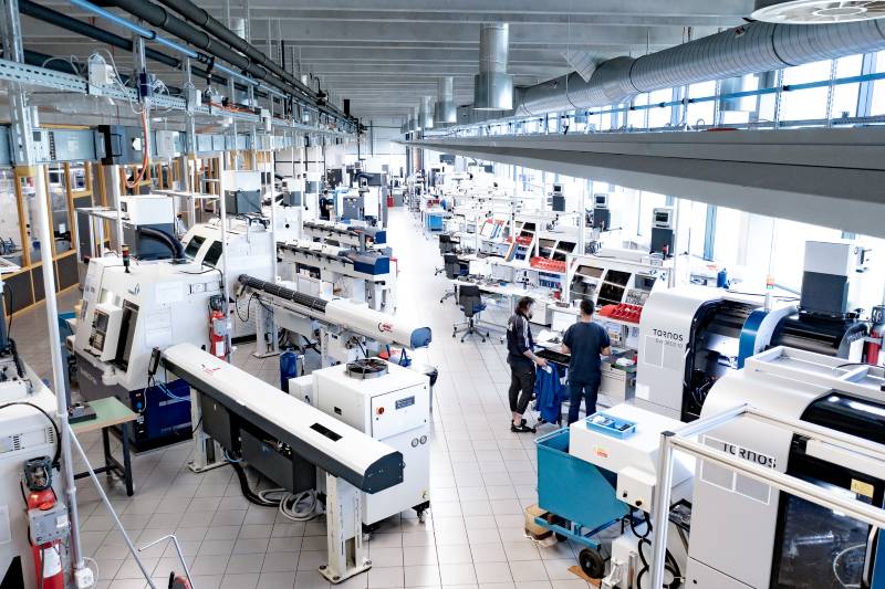
Swiss precision engineering and manufacturing
In our extensive production halls, Swiss precision turning, milling, EDM, grinding, lapping, polishing and many other processes below to our core competences. Our engineers are always seeking to get the most out of our equipments to offer you the best possible solution. Thanks to this, we can achieve submicron dimensional precision and surface finishes of Ra < 0.1 µm.
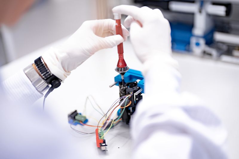
Reliable perfromance, ready for integration
We deliver you a working and tested system that integrates mechanism, actuation, and position feedback, and that has been validated against your requirements. We optimize the positioning accuracy, settling behaviour and service life according to your operating conditions. Mechanical, electrical and control interfaces are developed for your equipment, reducing the engineering work your team needs to carry out during integration.
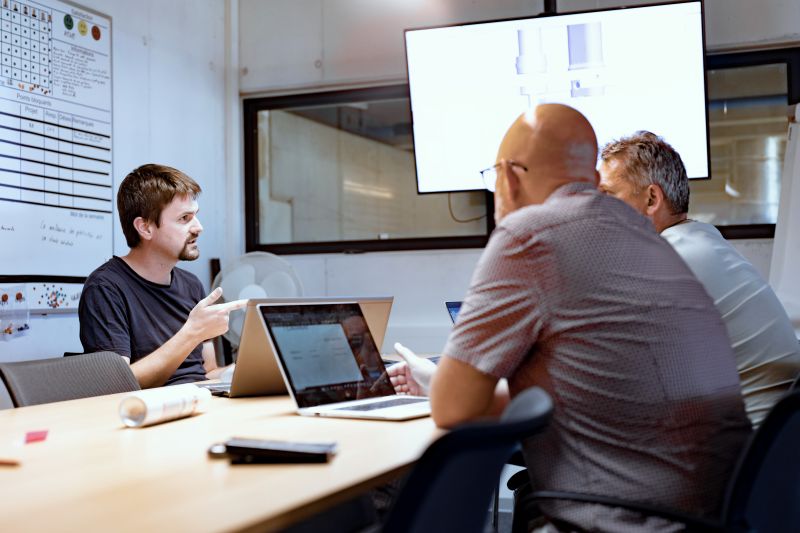
A committed partner throughout your product’s life
A dedicated project manager coordinates your project from the first technical discussions through industrialisation and series production. Regular project reviews cover progress, costs and decisions. When requirements prove difficult, we work through the options with you. Support continues throughout production, covering engineering changes, product improvements and planning for long-term supply.
Tell us what the part or subsystem needs to do, the conditions it will operate in and the production volumes you expect. We can review the requirements with your team and identify the engineering and manufacturing work needed.
Ivica Tolich
Business Development Manager - Semiconductor
+1 408 476 7973
Ivica.tolich(a)mpsag.com

Over the years, we have built up a large network of academic partners with whom we collaborate to develop state-of-the-art solutions.
• PSI - Paul Scherrer Institute
• EPFL - École Polytechnique Fédérale Lausanne
• ETHZ - Eidgenössische technische Hochschule Zürich
• HES-SO - Haute école supérieure de Suisse occidentale
• OST - Ostschweizer Hochschule
• University of Berne
• CSEM - Centre Suisse d'Électronique et de Microtechnique
• EMPA - Swiss Federal Laboratories for Materials Testing and Research